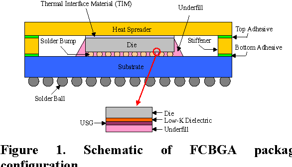
Design Guidance for the Mechanical Reliability of Low-K Flip Chip BGA Package
@inproceedings{Chang2004DesignGF,
  title={Design Guidance for the Mechanical Reliability of Low-K Flip Chip BGA Package},
  author={Kuo-Chin Chang and Yuan Li and Chung-yi Lin and M. J. Lii},
  year={2004},
  url={https://api.semanticscholar.org/CorpusID:17892454}
}Flip Chip Ball Grid Array (FCBGA) package has been introduced in recent years to address the needs in the microelectronic packaging industry for increasing performance and I/O density, which offers a cost effective solution with smaller form factor. Furthermore, Cu interconnects with low-k dielectric material were also introduced to reduce power consumption and further enhance device performance. Due to the nature of low-k dielectric material characteristics, it is more sensitive while a…
No Paper Link Available
Figures and Tables from this paper
27 Citations
A Novel Metal Scheme and Bump Array Design Configuration to Enhance Advanced Si Packages CPI Reliability Performance by Using Finite Element Modeling Technique
- 2019
Engineering, Materials Science
Flip chip packages with Cu bump have been introduced in recent years to address the needs of advanced packaging for reducing bump pitch and increasing I/O density, which can also enhance performance…
Thermal behavior analysis of lead-free flip-chip ball grid array packages with different underfill material properties
- 2008
Engineering, Materials Science
Low-k materials have been introduced in the backend interconnects since 90 nm node for advanced microelectronic products in order to reduce the RC delay. However, the fragile low-k layer is very…
ADVANCED SIMULATION/MODELING AND RELIABILITY OF FINE PITCH (130um) LEAD- FREE FLIP-CHIP PACKAGE
- 2008
Engineering, Materials Science
Flip-chip technology has been introduced in recent years which accommodate the ever increasing demands for higher performance and I/O density, while achieving smaller form factor and offering a cost…
Challenges of Thin Core Substrate Flip Chip Package on Advanced Si Nodes
- 2007
Engineering, Materials Science
Advanced silicon node is becoming the mainstream technology used for electronic product and flip chip package is one of the assembly solutions to meet of high-end products requirement. For flip-chip…
Reliability of fine-pitch flip-chip packages
- 2009
Engineering, Materials Science
A new low-cost flip-chip technology that leverages the existing fine pitch flip-chip technologies is discussed. For decades, the C4 process has served as the main interconnect method in the flip-chip…
A Novel Stacked-via Cu/ELK Interconnection Design Configuration to Enhance Advanced Si Packages Reliability Performance
- 2023
Engineering, Materials Science
In recent years, stacked-via Cu interconnect with extra low-k (ELK) dielectric material had been applied to reduce power consumption and further enhance device performance, especially for advanced…
Effect of Underfill Mechanical Property on Cu/Low-K Delamination for Lead-Free Flip Chip Packaging
- 2008
Engineering, Materials Science
The low dielectric constant (low-K) material and copper (Cu) interconnection in chip enhance the electrical speed for microelectronic devices. The low-K materials generally show low mechanical…
Lead-Free Flip-Chip Packaging Affects on Ultralow-$k$ Chip Delamination
- 2012
Engineering, Materials Science
Ultralow-k dielectric materials generally show weak mechanical strength (E <; 8 GPa), a high coefficient of thermal expansion (5 ppm/°C-8 ppm/°C), and poor adhesion ( <; 5 J/m2-10 J/m2). As a result,…
Analysis of Thermal Stress and Its Influence on Carrier Mobility in Three-Dimensional Microelectronic Chip Stack
- 2015
Engineering, Materials Science
A numerical assessment on the thermal stress in a three-dimensional (3D) microelectronic package structure is performed. The objectives are to study how the chip stack/microbump assembly responds to…
Copper pillar bump design optimization for lead free flip-chip packaging
- 2010
Engineering, Materials Science
The interfacial delamination between the under bump metallurgy and the aluminum (Al) pad was observed in a copper (Cu) pillar bump evaluation in the work. The finite element analysis was employed to…
9 References
Impact of flip-chip packaging on copper/low-k structures
- 2003
Engineering, Materials Science
Copper/low-k structures are the desired choice for advanced integrated circuits (ICs). Nevertheless, the reliability might become a concern due to the considerably lower strength and greater…
Analysis of flip-chip packaging challenges on copper/low-k interconnects
- 2003
Engineering, Materials Science
An interfacial-fracture-mechanics-based simulation methodology has been developed to study the flip-chip packaging effect on the copper/low-k structures. Multilevel submodeling techniques have been…
Effect of packaging on interfacial cracking in Cu/ low k Damascene structures
- 2003
Engineering, Materials Science
In this study, 3D f~te element analysis (FEA) based on a multilevel sub-modeling approach in combination with highresolution moire interferometry was employed to examine the packaging effect on low k…
Interfacial adhesion study for copper/SiLK interconnects in flip-chip packages
- 2001
Materials Science, Engineering
This paper presents the results of a two-part study to determine the fracture toughness of relevant interfaces within Cu/SiLK low-k interconnect structures and relate those data to the actual driving…
Failure analysis of solder bumped flip chip on low-cost substrates
- 1999
Engineering, Materials Science
Failure analyses of 63wt%Sn-37wt%Pb solder bumped flip chip assemblies with underfill encapsulant are presented in this study. Emphasis is placed on solder flowed-out, nonuniform underfill and voids,…
Thermal stress and debonding in Cu/low k damascene line structures
- 2002
Engineering, Materials Science
In this study, the thermal stress and debond characteristics of Cu damascene structures were investigated using X-ray diffraction and 3D finite element analysis (FEA). First, X-ray diffraction was…
Enhancement of flip-chip fatigue life by encapsulation
- 1991
Materials Science, Engineering
Encapsulation of controlled collapse chip connection (C4) joints, using a filled epoxy resin with a matched coefficient of thermal expansion (CTE), has provided a substantial increase in the life of…
Effects of dielectric material and linewidth on thermal stresses of Cu line structures
- 2002
Engineering, Materials Science
Thermal stresses of Cu line structures of 0.4 and 0.2 /spl mu/m linewidth integrated with fluorinated silicon oxide SiOF and two kinds of low k dielectrics, carbon doped oxide CDO and organic polymer…